Products

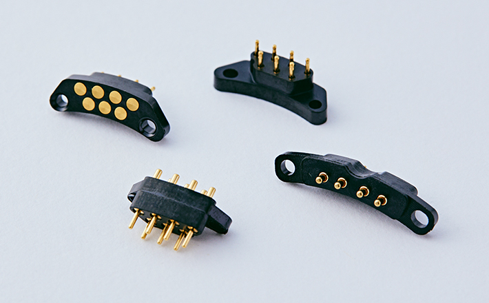
- Coaxial Structure Socket for mm-wave Device
- Antenna in Package (AiP) Socket
- FPGA Socket
- Multi Impedance Socket
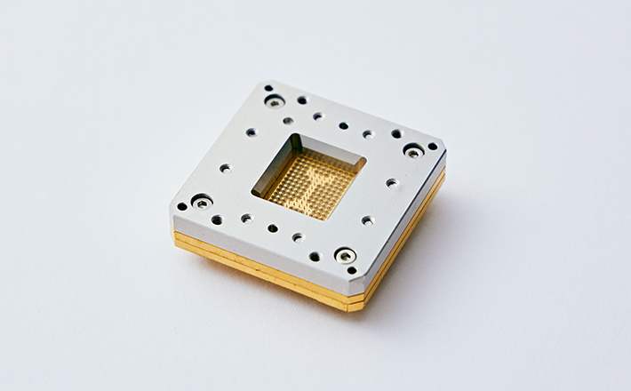
- Image Sensor Socket
- High Speed Signal Probing Socket
- Product Board Socket (YOROI)
- Probe Card Socket for WLCSP
- Socket for BGA・LGA
- Crystal・MEMS Device Socket
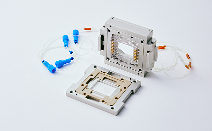
- Microfluidics Interface Unit (RYURO)